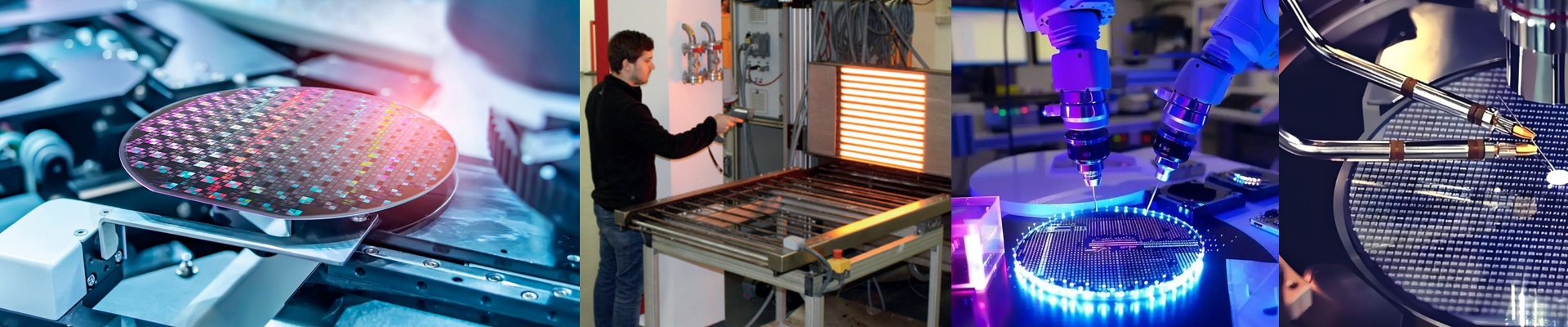
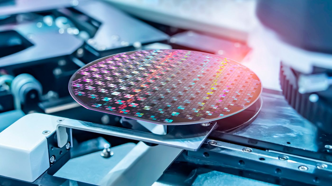
On the fab floor, a 0.1°C drift in bake temperature can move a critical dimension by nanometers. That shift means scrapped wafers, shrunk photoresist margin, and yield pressure that doesn’t quit.
What matters, technically
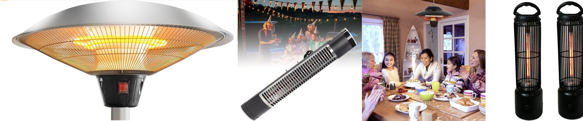
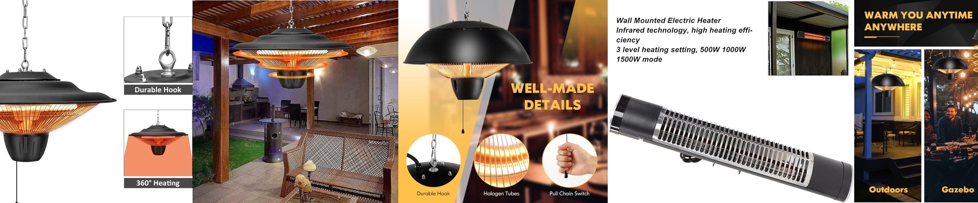
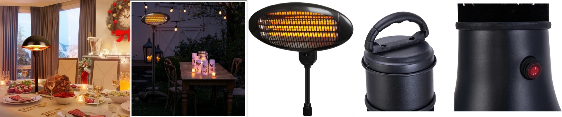
We built the linear infrared heating emitter around semiconductor thermal budgets. It throws rapid, direct-coupled NIR energy at the wafer and holds uniformity within ±0.1°C across the active zone, so soft bake and hard bake profiles repeat—shot after shot. It runs clean in Class 1–100 environments: zero particle generation, and a sealed architecture that keeps contamination where it belongs—outside the process zone. Output stays stable under continuous duty. Field data shows 5,000+ hours at constant setpoint with minimal decay. The design lines up with international semiconductor equipment norms and gives you a validated, equivalent replacement path. Integration is mechanical and electrical—no guesswork.
Why it works in lithography
Photoresist response is about temperature history, not just the peak. Our linear emitter heats fast, cools fast, and repeats the same thermal profile consistently. That means fewer reworks, tighter CD control, and cycle time you can plan around. Energy use drops because there’s minimal thermal mass—heat on demand, no warm-up penalty. Uptime follows. The system is built for 24/7 operation with predictable maintenance intervals, and the clean output keeps particle counts low where it matters most: on the wafer.
What you need to know
Installation comes down to precise optical alignment and a dedicated, low-noise power supply matched to the emitter’s voltage and current profile. Thermal crosstalk is real if the emitter sits too close to adjacent modules. We provide clearance maps and thermal shielding guidance to preserve uniformity. And if your process cycles between bake and cool, make sure your chiller can keep pace. The emitter will deliver the heat; the full profile still depends on the surrounding thermal system.